
The 2N3055 is a power bipolar transistor designed to handle high power loads in the range of 100 V, and 15 amps.
In this post I will comprehensively discuss the pinout function, electrical specification, and application designs for the power transistor 2N3055.
If you are an electronic hobbyist, you might have certainly used this very useful, and efficient power transistor at least once in your experiments. I have used 2N3055 transistor many number of times in many of my high current circuit applications without any issues.
Main Features
- DC Current Gain or hFE = 20 −70 @ IC = 4 Amps (Collector Current)
- Collector−Emitter Saturation Voltage − VCE(sat) = 1.1 Vdc (Max) @ IC = 4 Adc
- Outstanding Safe Operating Area
- Available with Pb−Free Packages
Pinout Diagram
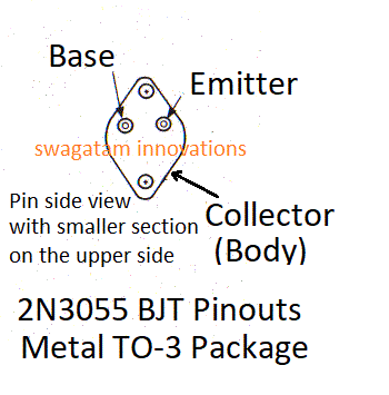
How to Connect the Pinouts
Just like any other npn BJT, 2N3055 connections are also pretty straightforward. In the common emitter mode which is most frequently used configuration, the emitter pin is connected with the ground line or the negative supply line.
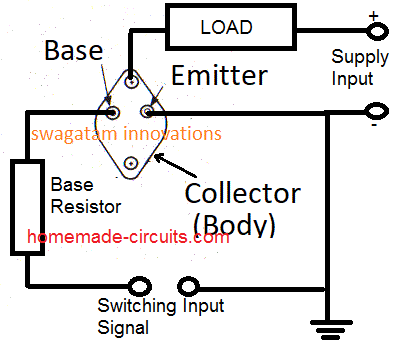
The base is connected across the input signal through which the transistor needs to be switched ON or OFF. This input switching signal can be anywhere between 1V and 12V ideally. A calculated resistor must be included in series with the base pinout of the transistor.
The base resistor value will depend on the load specifications attached at the collector pin of the transistor. The basic formula can be studied from this article.
The collector pin should be connected with one terminal of the load, while the other terminal connects with the positive supply line. The load current specs must be at any cost lower than 15 amps, in fact lower than 14 amps to avoid current reaching the breakdown limit.
MAXIMUM RATINGS AND SPECIFICATIONS OF 2N3055 TRANSISTOR
Maximum ratings are the highest tolerable values beyond which a permanent damage can occur to the device. These ratings specified to the device are stress limit values (not the standard operating criteria) for the particular device and are not valid simultaneously.
If these limits are exceeded, device may cease to function with its standard specifications, causing severe damage to the device and also affecting its reliability parameters.
- Collector to Emitter Voltage VCER = 70 Vdc
- Collector to Base Voltage VCB = 100 Vdc
- Emitter to Base Voltage VEB = 7 Vdc
- Continuous Collector-Current IC = 15 Adc
- Base Current IB = 7 Adc
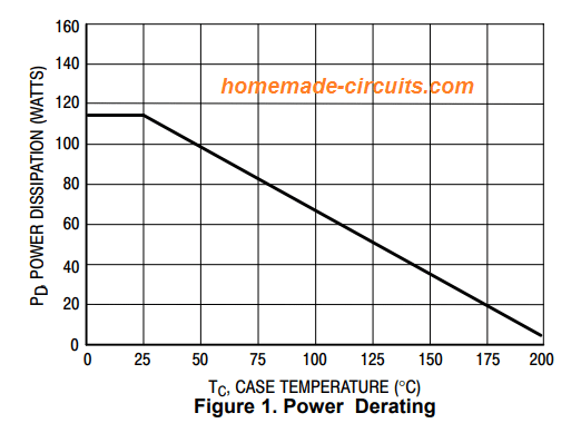
- Total Power Dissipation @ TC = 25°C Derate Above 25°C PD = 115 W @ 0.657 W/°C
- Operating and Storage Junction Temperature Range TJ, Tstg = − 65 to +200 °C
THERMAL CHARACTERISTICS of 2N3055
Thermal Resistance from Junction−to−Case R0JC = 1.52 C/W
ELECTRICAL CHARACTERISTICS of 2N3055(TC = 25 C unless otherwise specified)
CHARACTERISTICS WHEN DEVICE IS OFF
- Collector−Emitter Sustaining Voltage at collector current IC = 200 mAdc, IB = 0) VCEO(sus) = 60 Vdc
- Collector−Emitter Sustaining Voltage at collector current IC = 200 mAdc, RBE = 100 fi) VCER(sus) = 70 Vdc
- Collector Cutoff Current (VCE = 30 Vdc, IB = 0) ICEO = 0.7 mA
- Collector Cutoff Current (VCE = 100 Vdc, VBE(off) = 1.5 Vdc) ICEX = 1.0 mA
- Emitter Cutoff Current (VBE = 7.0 Vdc, IC = 0) IEBO = 5.0 mA
CHARACTERISTICS WHEN DEVICE IS ON
- DC Current Gain (IC = 4.0 Adc, VCE = 4.0 Vdc) (IC = 10 Adc, VCE = 4.0 Vdc) hFE = 20 to 70
- Collector−Emitter Saturation Voltage (IC = 4.0 Adc, IB = 400 mAdc) (IC = 10 Adc, IB = 3.3 Adc) VCE(sat) = 1.1 to 3 Vdc
- Base−Emitter On Voltage (IC = 4.0 Adc, VCE = 4.0 Vdc) VBE(on) = 1.5 Vdc
DYNAMIC CHARACTERISTICS
- Current Gain − Bandwidth Product (IC = 0.5 Adc, VCE = 10 Vdc, f = 1.0 MHz) fT = 2.5 MHz
- *Small−Signal Current Gain (IC = 1.0 Adc, VCE = 4.0 Vdc, f = 1.0 kHz) hfe = 15 to 120
- *Small−Signal Current Gain Cutoff Frequency (VCE = 4.0 Vdc, IC = 1.0 Adc, f = 1.0 kHz) f hfe = 10 kHz
- *Indicates Within JEDEC Registration. (2N3055)
The transistor comes with a couple of limitations in terms power handling capability.
- Average junction temperature
- Breakdown voltage
Safe operating area curves indicate the IC − VCE limits of the 2N3055 transistor that must be taken care of in order to ensure a stable and error free operation. Meaning the transistor must not be operated to increased dissipation levels than what is advised in the curves traces.
The data given in the figure below is plotted while TC = 25°C; TJ(pk) is variable in accordance with the power level.
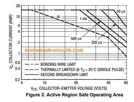
Second breakdown pulse boundaries are legitimate for duty cycles upto 10% but must be derated for temperatures as indicated in the following figure:
Application Circuits using 2N3055
The 2N3055 is a versatile NPN power transistor which can be effectively applied for all medium power (current) delivering circuit. The few main of these applications are in the field of inverters and power amplifiers. Due to relatively high hFE range this device can be used in a wide range of circuits for handling high current efficiently.
It's metal TO3 case becomes ideally suited for attaching a fast cooling large heatsink quickly and easily allowing the device to work in its most favorable conditions.
I have plenty of 2N3055 based circuits in this website, glad to present a few of them here.
Amplifier Circuit using a single 2N3055
The circuit is the most basic form of power amplifier which can be build using a single 2N3055 BJT.
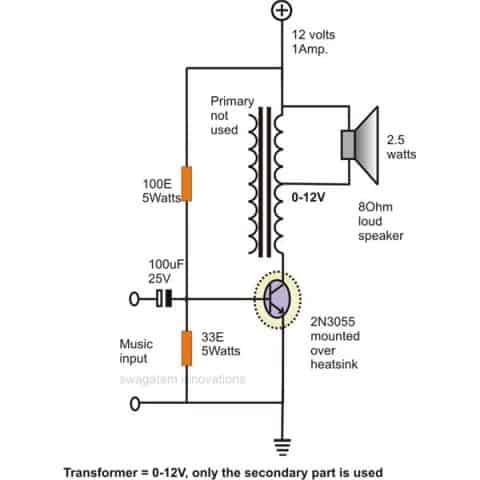
Although the amplifier above looks too simple to make, the low-tech design forces the 2N3055 to dissipate a lot power through heat.
For a more efficient and Hi-Fi amplifier design, I recommend the following mini crescendo, which is perhaps one of the most classic and efficient amplifier circuits using just a pair of 2N3055 transistors. For complete details you can read this article

Tiniest Inverter using 2N3055
I am sure you might have already come across this little inverter circuit. This circuit using only two 2N3055 and a transformer for creating a reasonably powered 60 to 100 watt 50 Hz power inverter. An ideal project for all new hobbyists and school students.
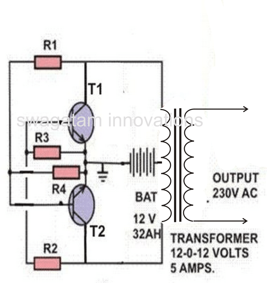
R1, R2= 100 OHMS./ 10 WATTS WIRE WOUND
R3, R4= 15 OHMS/ 10 WATTS WIRE WOUND
T1, T2 = 2N3055 POWER TRANSISTORS
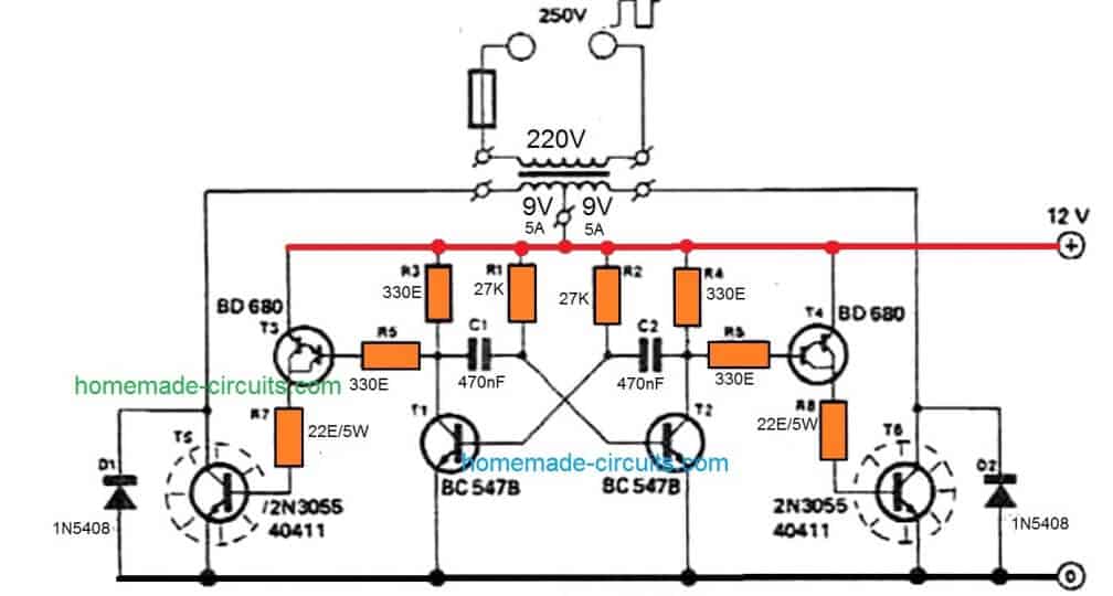
Power Inverter 100 watts using 2N3055
If you are not satisfied with the power output from the above design, you can always upgrade it to a full-fledged, 100 to 500 watt power inverter, using a single or many 2N3055 transistors in parallel, as shown below:
Variable Power Supply Circuit using 2N3055
An awesome easy to build variable voltage and current work bench power supply can be built quickly using a single 2N3055 transistor and a few other complementing components, as shown below:
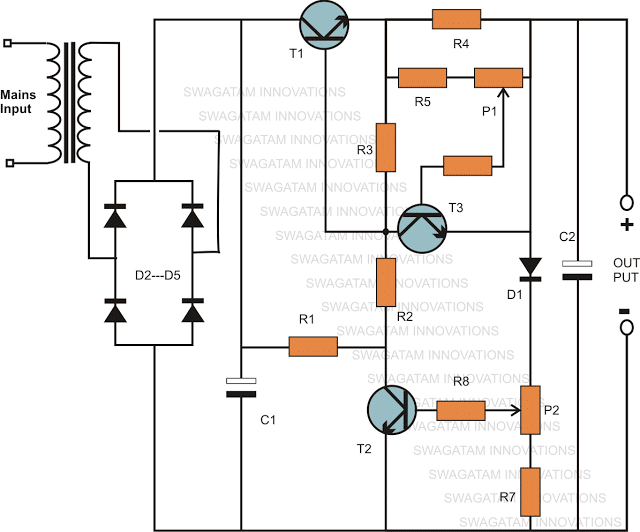
For more description and parts list you can visit this post
12V to 48V Battery Charger using 2N3055

This simple automatic 2N3055 based battery charger circuit can be used for charging any lead acid battery from 12V to 48V.
The high current handling capacity upto 7 amps of this device will allow an ideal, charging for any battery from 7 Ah to 150 Ah using the above circuit.
It has an automatic cut-off feature which will never allow the battery to get over charged.
Conclusion
From the above posting I have explained the main specifications and datasheet of the versatile workhorse transistor 2N3055.
This transistor is a universal power BJT that can be used in almost all higher power based applications where high current and efficient switching of current is expected.
The maximum voltage this device can handle is 70V which looks very impressive, and a continuous current for around 15 amp, when the device is mounted over a well ventilated heatsink.
We also studied a few cool application circuits using 2N3055, and how to connect it through its pinout diagram.
If you have any further doubts please use the comment box below for interacting.