In this post we learn how to make a simple transistor latch circuit using just two BJTs and a few resistors.
Introduction
A transistor latch is a circuit which latches ON with a permanent high output in response to a momentary input high signal, and continues to stay in this position as long as its in the powered condition, regardless of the input signal.
A latch circuit can be used to lock or latch the output of the circuit in response to an input signal and sustain the position even after the input signal is removed.
The output may be used to operate a load controlled through a relay, SCR, Triac or simply by the output transistor itself.
Working Description:
The simple latch circuit using transistors described in this article can be made very cheaply using just a couple of transistors and some other passive component.

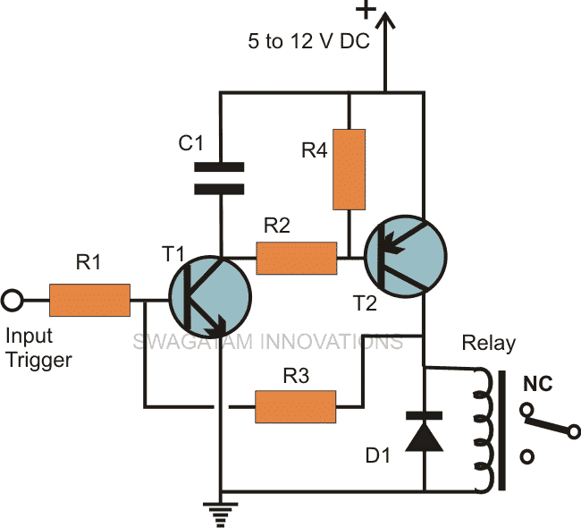
As shown in the figure transistor T1 and T2 are configured in such a manner that T2 follows T1 to either conduct and or to stop the conduction depending upon the trigger received at the input of T1.
T2 also acts as a buffer and produces better response even to very small signals.
When a small positive signal is applied at the input of T1, T1 instantly conducts and pulls the base of T2 to ground.
This initiates T2 which also starts conducting with the received negative biasing offered by the conduction of T1.
It must be noted here that T being NPN device responds to positive signals while T2 being a PNP responds to negative potential generated by the conduction of T1.
Uptill here the function looks pretty ordinary as we witness a very normal and obvious transistor functioning.
How the Feedback from R3 Works to Latch the Circuit
However the introduction of a feedback voltage through R3 makes a huge difference to the configuration and helps to generate the required feature in the circuit, that is the BJT circuit instantly latches or freezes its output with a constant positive supply.
If a relay is used here it would also operate and stay in that position even after the input trigger is completely removed.
The moment T2 follows T1, R3 connects or feeds back some voltage from the collector of T2 back to the base of T1 making it conduct virtually “for ever”.
C1 prevents the circuit from getting activated with false triggers generated from stray pick-ups, and during switch ON transients.
The situation can be restored back either by restarting power to the circuit or by grounding the base of T1 through a push button arrangement.
The circuit can be used for many important applications, especially in security systems and in alarm systems.
Calculating Transistor Biasing
It can done with the following formulas
VBE = 0.7V
IE = (β + 1)IB ≅ IC
IC = βIB
Testing procedure can seen in the following video tutorial:

Parts List
- R1, R2, R4 = 10K,
- R3 = 100K,
- T1 = BC547,
- T2 = BC557
- C1 = 1uF/25V
- D1 = 1N4007,
- Relay = As preferred.
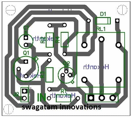
PCB Design