SSR or Solid state relays are high power electrical switches that work without involving mechanical contacts, instead they use solid state semiconductors like MOSFETs for switching an electrical load.
SSRs can be used for operating high power loads, through a small input trigger voltage with negligible current.
These devices can be used for operating high power AC loads as well as DC loads.
Solid State Relays are highly efficient compared to the electro-mechanical relays due to a few distinct features.
Main Features and Advantages of SSR
The main features and advantages of solid state relays or SSRs are:
- SSRs can be built easily using a minimum number ordinary electronic parts
- They work without any form of clicking sound due to the absence of mechanical contacts.
- Being solid state also means SSRs can switch at much faster speed than the traditional electro-mechanical types.
- SSRs do not depend external supply for switching ON, rather extract the supply from the load itself.
- They work using negligible current and therefore do not drain battery in battery operated systems. This also ensures negligible idle current for the device.
Basic SSR Working Concept using MOSFETs
In one of my earlier posts I explained how a MOSFET based bidirectional switch could be used for operating any desired electrical load, just like a standard mechanical switch , but with exceptional advantages.
The same MOSFET bidirectional switch concept could be applied for making an ideal SSR device.
For a Triac based SSR please refer to this post
Basic SSR Design
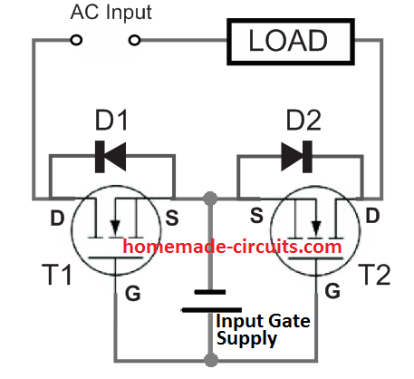
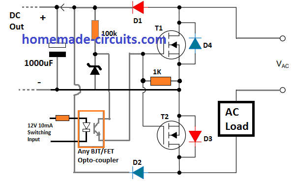
In the above shown basic SSR design, we can see a couple of appropriately rated MOSFETs T1 and T2 connected back to back with their source and gate terminals joined in common with each other.
D1 and D2 are internal body diodes across the drain/source of the respective MOSFETs.
An input DC supply can also be seen attached across the common gate/source terminals of the two MOSFETs. This supply is used for triggering the MOSFETs ON or for enabling permanent switch ON for the MOSFETs while the SSR unit is operational.
The AC supply which could be up to grid mains level and the load are connected in series across the two drains of the MOSFETs.
How it Works
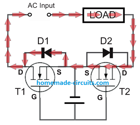
The working of the proposed sold state relay can be understood by referring to the following diagram, and the corresponding details:
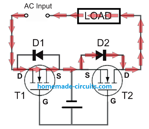
With the above setup, due to the input gate supply connected, T1 and T2 are both in the switched ON position. When the load side AC input is switch ON, the left diagram shows how the positive half cycle conducts through the relevant MOSFET/diode pair (T1, D2) and the right side diagram shows how the negative AC cycle conducts through the other complementing MOSFET/diode pair (T2, D1).
In the left diagram we find one of the AC half cycles goes through T1, and D2 (T2 being reverse biased), and finally completes the cycle via the load.
The right side diagram shows how the other half cycle completes the circuit in the opposite direction by conducting through the load, T2, D1 (T1 being reversed biased in this case).
In this way the two MOSFETs T1, T2 along with their respective drain/source body diodes D1, D2, allow both the half cycles of the AC to conduct, powering the AC load perfectly, and accomplishing the SSR role efficiently.
Here's an excerpt from the datasheet of the article.

Video showing the testing of the above SSR circuit
Making a Practical SSR Circuit
So far we have learned the theoretical design of an SSR, now let's move ahead and see how a practical solid state relay module could be built, for switching a desired high power AC load, without any external input DC.
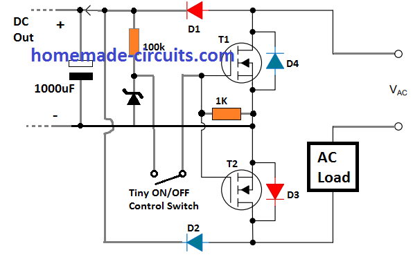
The above SSR circuit is configured exactly in the same way as discussed in the earlier basic design. However, here we find two additional diodes D1, and D2, along with the MOSFET internal body diodes D3, D4.
The diodes D1, D2 are introduced for a specific purpose such that it forms a bridge rectifier in conjunction with the D3, D4 MOSFET body diodes.
The tiny on OFF switch could be used for turning the SSR ON/OFF. This switch could be a reed switch or any low current switch.
For high speed switching you can replace the switch with a opto-coupler as shown below.
In essence the circuit now fulfills 3 requirements.
- It powers the AC load through the MOSFET/Diode SSR configuration.
- The bridge rectifier formed by D1---D4 simultaneously converts the load AC input into rectified and filtered DC, and this DC is used for biasing the gates of the MOSFETs. This allows the MOSFETs to get appropriately turned ON through the load AC itself, without depending on any external DC.
- The rectified DC is further terminated as an auxiliary DC output which could be used for powering any suitable external load.
Circuit Problem
A closer look at the above design suggests that, this SSR design might have problems implementing the intended function efficiently. This is because, the moment the switching DC arrives at the gate of the MOSFET, it will begin turning ON, causing a bypassing of the current through the drain/source, depleting the gate/source voltage.
Let's consider the MOSFET T1. As soon as the rectified DC begins reaching the gate of T1, it will begin turning ON right from around 4 V onward, causing a bypassing effect of the the supply via its drain/source terminals. During this moment, the DC will struggle to rise across the zener diode and begin dropping toward zero.
This will in turn cause the MOSFET to turn OFF, and the continuous stale-mate kind of struggle or a tug of war will occur between the MOSFET drain/source and the MOSFET gate/source, preventing the SSR from functioning correctly.
The Solution
The solution to the above issue could be accomplished using the following example circuit concept.
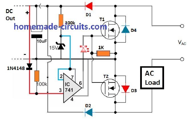
The objective here is, to make sure that the MOSFETs do not conduct until an optimum 15 V is developed across the zener diode, or across the gate/source of the MOSFETs
The op amp ensures that its output fires only once the DC line crosses the 15 V zener diode reference threshold, which allows the MOSFET gates to get an optimal 15 V DC for the conduction.
The red line associated with pin3 of IC 741 can be toggled through an opto coupler for the required switching from an external source.
How it Works: As we can see, the inverting input of the op amp is tied with the 15V zener, which forms a reference level for the op amp pin2. Pin3 which is the non-inverting input of the op amp is connected with the positive line. This configuration ensures that the output pin6 of the op amp produces a 15V supply only once its pin3 voltage reaches above 15 V mark The action ensures that the MOSFETs conduct only through a valid 15 V optimal gate voltage, enabling a proper working of the SSR.
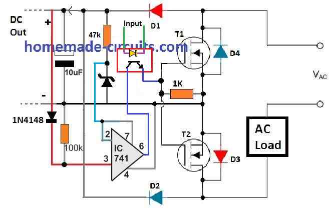
Isolated Switching
The main feature of any SSR is to enable the user an isolated switching of the device through an external signal.
The above op amp based design could be facilitated with this feature as demonstrated in the following concept:
How the Diodes Work Like Bridge Rectifier
During the positive half cycles, the current moves through D1, 100k, zener, D3 and back to the AC source.
During the other half cycle, the current moves through D2, 100k, zener, D4 and back to the AC source.
Reference: SSR

Comments
Hello, I’m building/have built a circuit that takes a 50hz ac signal from a class ab amplifier circuit and puts it as the ac input to a n channel fet relay as per fig. 3 above. I’m using a fod 3180 as the driver for the fet’s and so far everything works fine. Where I’m having issues is that I’m using a 555 timer to turn on and off the fod 3180 at about 1khz. On the positive half of the cycle the ac is shut off as expected, as a series of steps up and down the waveform; however, the bottom half of the cycle is unaltered, it’s just a negative sine wave.
I have to admit I’m just about at my wits end on this one. Do you have any idea why the negative half cycle doesn’t turn on and off like the positive half?
Thanks for any help you may provide.
Hi, did you connect the sources of the two MOSFETs with the negative (ground) of the IC 555? And I think a MOSFET driver is not required…you can directly feed the pin#3 of Ic 555 with the gates of the two MOSFETs
Hi Swagatam,
No, I didn’t connect the sources to the neutral ground and I used the driver because I thought that I read in the article that when you use N-channel FETs a driver is necessary in order to charge and discharge the gates of the FETs.
Thanks for the advice, I’ll try it and see how that works out. I’ll let you know if it works.
….I think you are right….a gate driver is strictly required for this application.
Please refer to the following post and check the following and read the “Using N-Channel MOSFET” section:
https://www.homemade-circuits.com/bidirectional-switch/
No problem Kurt,
Initially just connect the pin#3 of the IC 555 with the common gates of the MOSFETs, and connect the common sources with the negative or ground of the 555 circuit, also make sure to connect a 1k resistor between the gates and sources of the MOSFETs. A driver is necessary only when the load current is very high…
hie this diagrams are using DC 12v to genarate AC . can you provide me with a diagram which uses DC 400v to genarate AC . thanks
This circuit is not generating AC, it is controlling an AC load.
Hi, having minimal knowledge of electronics, I was wondering if the final circuit would be able to work safely on 240VAC power input and an 800W resistive load.
Hi, the above concepts are recommended only for experts in the field, not for newcomers, so I won’t recommend it to you.
If your load is a resistive load, then it can be simply controlled through a single MOSFET and a bridge rectifier, no need of the above complex design. Let me know if you would like to see the full schematic.
I have a 3d printer hotbed (resistive load 4 x 200W) and this should be controlled using PWM. So I was trying to find a solution for that, and discovered you article which seemed fit for my case. If you think that another simpler circuit, could make it work, I would like to have the schematic.
In any case, thank you for responding!
I think you should try a dimmer switch circuit such as this for PWM controlling of your load:
https://www.homemade-circuits.com/simple-ceiling-fan-regulator-circuit/
Your diagram is completely wrong. I don’t think you know what you’re talking about at all. When the MOSFET is on, current flows through the channel, not the body diode.
I know the current flows through the channel, the main thing is that, does the above concept work as intended in the application, or not.
Hi , I have a question .Is there anywhere I can find a Power mosfet Solid State relay for 20 amps using 120 VAC for sale or at least PCB kit ,maybe even pcb layout with , if possible a GERBER file, so I can order the production of a prototype Mosfet SSr for A C ?
Thanks in advance
Hi, you can try the following modified version of the first circuit:
https://www.homemade-circuits.com/wp-content/uploads/2024/05/simple-mosfet-AC-220V-ssr-circuit.jpg
However, I do not have the PCB details for this design.
Thank you very much !!
Hi sir, hope all is going well. Sir i need your
kind support. I want to make 40amp ssr.can you provide me diagram with components plz as usual in easy way plz
Hi Ghulam, what type of load do to want to control with the SSR, AC load or DC load?
Sir i want to run AC load, i tried with bt136, but as you know bt136 can’t handle heavy load…..i have bta41 800B. So plz guide me with diagram and components which is required. Plz
Thanks
Hi Ghulam, yes you can use BTA41800, it is rated to handle 40 amps load.
I hope you are referring to the following design
https://www.homemade-circuits.com/wp-content/uploads/2021/06/MOC3040-SSR-circuit-compressed.jpg
Yes sir same i want, sir what is the value of R1?all resister required qaurter watt? Sir can i use moc3021?sir plz guide me with diagram of bta41 800b. I dont have TIC 226 D/M plz
Thanks
Ghulam, R1 can be 1k 1/4 watt if the input voltage is between 5v and 15V.
All other resistors can be 1 watt CFR.
Yes MOC3021 can be also used.
The shown triac can be replaced with your specific 40 amp triac, no issues.
MT1 will go to the R4 side and MT2 will go to the R2 side.
Thank you sir, i will try and update you.
Sure, no problem, Ghulam.
Hello Sir, great document Thank you for everything.
I have a question please, can we use the basic circuit to connect or disconnect a series of 200v photo voltaic panels?
Thank you again sir
Thank you Laurent, you can use the basic circuit to connect or disconnect PV panels, however the above circuits are meant for AC supplies and loads, for DC supplies, like from a PV systems, you can employ a simpler design using a single MOSFET.
Hi , my name is Helder , I am trying to find power Mosfets S S Rs, for a project where I can’t use Triac SSRs, maybe I am looking at wrong places , I just can’t find MOSFET SSRs for A C voltages on AC currents like 10 to 15 amps , any help would be greatly appreciated
Hello Helder, the circuit explained in the above articles specifically designed to handle AC inputs, so you can use the above circuits with AC supply and AC loads.
One minor issue with the explanation of the circuit is whether or not current is conducted mainly through the body diode in the “reverse” MOSFET or whether it goes through the channel. Your second figure suggests that this current goes through the body diode but in most practical circuits, it won’t. The channel of a MOSFET can conduct in both directions when the gate is appropriately biased. Placing a voltage on the gate creates a conducting channel between the drain and source which acts like a low-value resistor. If your gate drive is adequate for the MOSFETs involved and they are sized appropriately for the current, the forward drop across the channel resistance is likely to be far lower than the forward voltage of the body diode, so the diode won’t turn on and will pass negligible current whilst the vast majority of it passes the the channel just like it does in the “forward” MOSFET.
Thank you for your quick response. Sorry to hear you haven’t yet designed one. If and when you do, will I be sent an email letting me know?
No problem! Sure, I will!
Interesting subject. Thank you for requesting questions.
Magnetic switches are essential for power equipment safety (table saws etc). Much of the older equipment, that is still effective, continues to be used but are not so equipped. Magnetic switches are expensive and, I’m sure, could be replaced my electronic ones. Have you designed/made such a switch that might be used for 120v or 240v single phase circuits?
Hall effect sensor and reed relay are the electronic magnetic sensors, but they require an additional electronic circuit to work. I haven’t yet designed a specific circuit using these sensors for the mentioned application.
¡ Exelent articule !
Sure, No problem!
Thank you for giving the details about the connections.
I’ll let you the know the results for this and/or if I face any issue I will ask in comment section.
In the following circuit, remove the 15K resistors, and connect the 6 V or 12V AC secondary wires of the transformer with BA159 anode and the common line which connects with the ground side of the 47uF capacitor, and the 12 V zener diode anode.
https://cdn.hackaday.io/images/54431494705050322.png
Ok, can you provide me a reference circuit diagram for testing with a transformer.
Thank you
If a bridge rectifier is used then the there would be no issues according to me. Still, you can try confirming the present diagram through a transformer based power supply. If everything works OK then you can try the resistive transfomerless power supply with bridge rectifier.
Ok, I will try that. But what I’m thinking is still the -ve of the DC part has to be connected to source of the mosfet which in turn will be connected to node2 (phase/neutral) through Q2 body diode.
Thank you
If the ground connection looks confusing, then in that case you try a bridge rectifier instead of a single diode rectifier.
The alternate circuit you have provided is for discharging the gate of the mosfet more faster and also to protect the gate of the mosfet by adding gate resistor?
Also I have one doubt –
Example when there is a high pulse at D1, internal transistor will turn ON and external will be OFF. Due to that the mosfet will get high at its gate.
When there is low at D1, internal transistor will be OFF and external will be ON which will connect the gate of the mosfet to ground.
The ground is also connected to one of the mains terminal (phase/neutral) through the body diode of Q2.
In this same article you explained me that there is no harm because only ground is connected to one of the mains terminal and +ve part is not.
So when external transistor is ON the +12V is now connected to the same terminal of AC where ground is connected. Is this safe? If yes how?
Thank you in advance.
I completely missed that the optocoupler is being used for the PWM input. In that case a 1KHz frequency is quite a large frequency, and the R5 and R13 are very high values which must be reduced to 50 ohms. Or alternatively you can try modifying the setup in the following manner by adding an extra transistor:
https://www.homemade-circuits.com/wp-content/uploads/2023/05/bidirectional-switch-using-optocoupler.jpg
Okay.
Also there is no high frequency switching at the gate of the MOSFETs (only around 1KHz of PWM to drive the MOSFETs).
I have also read that for high frequency switching in order to provide a good turn on, turn off pulse & to reduce ringing a proper gate resistor is required.
So, as you said in my circuit it is not that important.
I will tinker with the circuit with what all discussion I had with you & will let you know.
Thanks a lot for your response.
The gate resistor and the gate diode may not be relevant for this diagram. The diode across the gate resistor is for enabling quick discharge of the MOSFET gate internal capacitance during the OFF periods of the gate switching frequency. But since here no frequency is used at the gates, it is a constant DC, the gate resistor and diode are not relevant and are not important.
The external diodes across the MOSFET drain/source is the only hope now and the TVS diode that you may be adding.
I’m using this circuit for my project——–
https://cdn.hackaday.io/images/54431494705050322.png
I’m not sure if the MOSFET is getting damaged due to surge current. It can be one possibility of surge current. I’m also going to add a fuse in series with the MOSFET (also given in the reference circuit). In my current design I’ve not added the fuse (fuse can protect the MOSFETs from surge current).
Also as you said, I’m going to add a series gate resistor for individual MOSFETs.
I want to know the purpose of connecting a reverse diode in series with the gate of the MOSFET.
I’m not able to select a proper MOV for protecting the Drain-source of the MOSFET.
So I’m planning to use a TVS diode for that by changing the MOSFET number. Currently I’m using IRF740 as mentioned in the reference diagram. I can also use IRF840 after checking its datasheet. Because with IRF840 I’m able to select a proper TVS diode in that range.
I have connected a 10k resistor between the gate & source of the MOSFETs.
As you said also will try by connecting an external diode parallel to body diode.
I’m trying to make this circuit better than the current version & your response is helping me a lot.
You are welcome Omkar, Is your MOSFETs blowing off due to surge current? I have not yet tested the above concept with 220V AC, I have tested it with 12 V AC only so i am not so sure about this situation. Also, calculating snubber can be quite tricky again, and I do not have the necessary formulas. Therefore I would recommend MOVs instead which are quite easy to determine.
Yes the clamping voltage can be below 400 V, maybe around 380 V, that might do the job. However if your MOSFETs are blowing without an MOV then that’s not a good thing. You can also try putting external diode across drain/source of the MOSFETs similar to the internal body diodes of the MOSFETs. I know putting external diodes does not make sense in this circuit since the MOSFETs can conduct both ways, still you can check the response by putting these external diodes whether these are able to provide any sort of avalanche protection.
I hope you have proper gate resistors installed with reverse diode, in series with the gates of the MOSFETs. Also make sure to have a 1K resistor installed across the gate/source of the MOSFETs.
Yes, selecting a proper TVS diode is a little tricky. Also thank you very much for your help till now.
I’m having one question regarding the protection of MOSFET & was reading your article – https://www.homemade-circuits.com/mosfet-protection-basics-explained-is/
While testing my circuit for AC light dimmer which uses two MOSFETs in series(in this way – https://www.homemade-circuits.com/wp-content/uploads/2020/01/SSR-concept.png), till now 2-3 times what happened is I’m getting a short across the drain & source of the MOSFET in both directions (forward & reverse bias of the internal diode).
In a new MOSFET, I get 0.5-0.7 V in forward bias & no reading in reverse bias which shows that the MOSFET is in good condition.
After replacing the MOSFET with a new one the circuit starts working again but I think this issue is nearby to avalanche protection mentioned in your article.
So, I think adding RC snubber/ MOV across the MOSFET would be a good idea. The max Vds voltage mentioned in the datasheet of IRF740 is 400V so need to select MOV around this voltage.
How can I calculate values of R & C to protect the MOSFET? Do you recommend any other type of components that can be used for protection?
Thank you in advance.
You are right, the clamping voltage should be close to the maximum permissible input voltage of the device. For example for your SMPS the breakdown down voltage of the TVS diode can be around 270V and the clamping voltage can be around 300 v, otherwise the TVS diode is not going to provide any protection to your SMPS
For P6KE350CA, the clamping voltage is still very high at around 482V.
For P6KE400CA, the clamping voltage is 548 V again too high.
I am seeing that the breakdown voltages are much lower than the clamping voltage, so i am not sure what should be near the maximum device voltage, the breakdown voltage or the clamping voltage?
The SMBJ188A has a clamping voltage of 304 V which looks good, but a breakdown voltage of around 209 V which is too low.
Thanks a lot for sharing this link, it is really helpful. Still I’m having one query. In some of my projects I’m using 5V-1A SMPS to power other electronics stuff & just want to make sure that the TVS diode recommended in their datasheet is proper for protection against any voltage spike. Till now 3-4 SMPS have stopped working and I’m assuming that TVS diode could be the reason for that.
The maximum AC input voltage given in the datasheet is 260V.
The recommended TVS diode given in the datasheet is P6KE550CA which is used to protect the input of the SMPS from any voltage spike.
1) The maximum clamping voltage given is 760V, what I understood is that if voltage spike appears then the TVS diode will clamp the voltage to 760V @ given Ipp and the SMPS will see 760V at its input. But the maximum input voltage for the SMPS is 260V, then is this safe for the SMPS? 2) The breakdown voltage given is 522.5V minimum. I read that breakdown voltage is the voltage at which the TVS diode starts to conduct/ starts protecting the circuit from spikes. For an example a voltage spike of 510V appears at the input of SMPS, because this voltage is less than 522.5 TVS diode will not start conducting as if it sees no voltage spike. But still 510V is greater than 260V, will it damage the SMPS? Can we use P6KE350CA/P6KE400CA to be more safe?
It is also written in the article that you shared the link for, that the clamping voltage should be nearby the working voltage of the device(considering some margin) to ensure more protection.
Thank you