Five simple yet effective electronic toggle flip flop switch circuits can be built around the IC 4017, IC 4093, and IC 4013. We will see how these can be implemented for switching a relay alternately ON OFF by alternately pressing a single push-button or through touch pads, which in turn will switch an electronic load such as fan, lights, or any similar appliance using a single push-button pressing.
What's a Flip Flop Circuit
A flip flop relay circuit works on a bistable circuit concept in which it has two stable stages either ON or OFF.
When used in practical applications circuits it allows a connected load to alternately toggle from an ON state to OFF state and vice versa in response to an external ON/OFF switching trigger through push button or touch pads.
So basically, it is a single push button relay ON/OFF circuit, which will alternately turn ON and OFF a relay and the connected load, in response to the alternate pressing of a push button or a touch pad.
In our following examples I have explained how to make a 4017 IC and 4093 IC based flip flop relay circuits.
These are designed to respond to alternate triggers through push-button, and correspondingly operate a relay and a load alternately from an ON state to OFF state and vice versa.
By adding just a handful of other passive components the circuit can be made to toggle accurately through subsequent input triggers either manually or electronically.
They may be operated through external triggers either manually or an electronic stage.
1) Simple Electronic Toggle Switch Flip Flop Circuit Using IC 4017
The first idea talks about an useful electronic flip flop toggle switch circuit built around the IC 4017. The component count here is minimum, and the result obtained is always up to the mark.
Referring to the figure we see that the IC is wired into its standard configuration, i.e. a logic high at its output shifts from one pin to the other in the influence of the applied clock at its pin # 14.
The alternate toggling at its clock input is recognized as clock pulses and is converted into the required toggling at its output pins. The whole operation may me understood with the following points:

Parts List
- R4 = 10K,
- R5 = 100K,
- R6, R7 = 4K7,
- C6, C7 = 10µF/25V,
- C8 = 1000µF/25V,
- C10 = 0.1, DISC,
- ALL DIODES ARE 1N4007,
- IC = 4017,
- T1 = BC 547, T2 = BC 557,
- IC2 = 7812
- TRANSFORMER = 0-12V, 500ma, INPUT AS PER AREA SPECIFICATIONS.
How it Works
We know that in response to every logic high pulse at pin #14, the output pins of the IC 4017 are switched high sequentially from # 3 to # 11 in the order: 3, 2, 4, 7, 1, 5, 6, 9, 10, and 11.
However, this proceeding may be stopped at any instant and repeated by just connecting any of the above pins to the reset pin # 15.
For example (in the present case), pin # 4 of the IC is connected to pin #15, therefore, sequence will be restricted and will bounce back to its initial position (pin # 3) each time the sequence (logic High) reaches pin # 4 and the cycle repeats.
It simply means that now the sequence toggles from pin # 3 to pin # 2 in a back and forth manner constituting a typical toggling action.
The operation of this electronic toggle switch circuit may be further understood as follows:
Every time a positive trigger is applied to the base of T1, it conducts and pulls down pin # 14 of the IC to ground. This brings the IC to a standby position.
The moment the trigger is removed, T1 stops conducting, pin # 14 now instantly receives a positive pulse from R1.
The IC acknowledges this as a clock signal and quickly toggles its output from its initial pin #3 to pin #2.
The next pulse produces the same result so that now the output shifts from pin #2 to pin #4, but since pin #4 is connected to reset pin #15, as explained, the situation bounces back to pin #3 (initial point).
Thus the procedure is repeated every time T1 receives a trigger either manually or through an external circuit.
Video Clip:
Upgrading the circuit to control more than one load
Now let's see how the above IC 4017 concept can be upgraded to operate 10 possible electrical loads through a single push button.
The idea was requested by Mr. Dheeraj.
Circuit Objectives and Requirements
I am Dhiraj Pathak from Assam, India.
As per the below diagram, following following operations should take place -
- The AC switch S1 when switched ON for the first time, AC load 1 should switch On and stay in ON state till S1 is witched OFF. AC load 2 should stay off during this operation
- The second time when S1 is again switched ON, AC Load 2 should switch ON and stay ON till S1 is switched OFF. AC load 1 should stay off during this operation
- The third time when S1 is again switched ON, both the AC loads should switch ON and stay ON till S1 is switched OFF.4. The fourth time when the S1 is switched ON , the operation cycle should repeat as mentioned in step 1, 2 and 3.
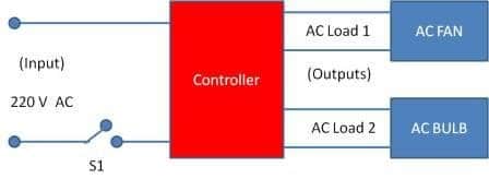
My intention is to use this design in my single living room of my rented apartment. The room has concealed wiring and the fan is located at the center of the roof.
The light will be connected parallel to the fan as a center light for the room. There is no extra power outlet at the center of the roof. Only outlet available is for the fan.
I do not wish to run separate wires from switchboard to the center light. Hence, I though of designing a logical circuit which can detect the state (On/OFF) of the power source and switch loads accordingly.
For using the center light, I do not wish to keep the fan ON all the time and vice versa.
Every time the circuit is powered ON, the last know state should trigger the next operation of the circuit.
The Design
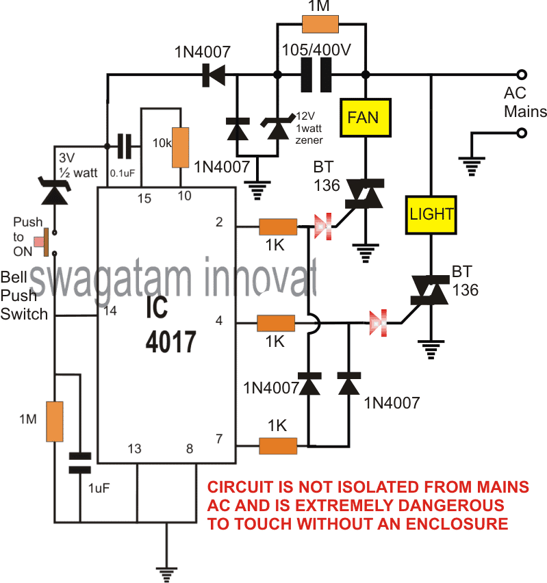
A simple electronic switch circuit customized to perform the above mentioned functions is shown below, without an MCU.
A bell push-button type switch is used for executing the sequential switching for the connected light and fan.
The design is self explanatory, if you have any doubts regarding the circuit description, please feel free to get it clarified through your comments.
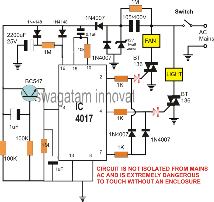
Electronic Switch without Push Button
As per the request and the feedback received from Mr. Dheeraj, the above design can be modified to work without a push button.... that is, using the existing ON/OFF switch at the mains input side for generating the specified toggling sequences.
The updated design can be witnessed in the below given figure:
Another interesting ON OFF relay witch with a single button can be configured using a single IC 4093. I have explained the procedures with the following explanation.
2) Accurate CMOS Flip Flop Circuit Using IC 4093
IC4093 Pinout Details
Parts List
- R3 = 10K,
- R4, R5 = 2M2,
- R6, R7 = 39K,
- C4, C5 = 0.22, DISC,
- C6 = 100µF/25V,
- D4, D5 = 1N4148,
- T1 = BC 547,
- IC = 4093,
The second concept is about a rather accurate circuit can be made using three gates of IC 4093. Looking at the figure we see that the inputs of N1 and N2 are joined together to form logic inverters, just like NOT gates.
It means that, any logic level applied to their inputs will be inverted at their outputs. Also, these two gates are connected in series to form a latch configuration with the help of a feedback loop via R5.
N1 and N2 will instantly latch the moment it senses a positive trigger at its input. Another gate N3 has been introduced basically to break this latch alternately after every subsequent input pulse.
The functioning of the circuit may be further understood with following explanation:
How it Works
On receiving a pulse at the trigger input, N1 quickly responds, its output changes state forcing N2 to also change state.
This causes the output of N2 to go high providing a feedback (via R5) to N1’s input and both the gates latch in that position.
At this position the output of N2 is locked at logic high, the preceding control circuit activates the relay and the connected load.
The high output also slowly charges C4, so that now one input of gate N3 becomes high. At this juncture, the other input of N3 is held at logic low by R7.
Now a pulse at the trigger point will make this input also go high momentarily, forcing its output to go low. This will pull the input of N1 to ground via D4, instantly breaking the latch.
This will make the output of N2 to go low, deactivating the transistor and the relay. The circuit is now back to its original state and ready for the next input trigger to repeat the entire procedure.
3) Flip Flop Circuit using IC 4013
The quick availability of the many CMOS ICs today has made designing of much complicated circuits a child's play, and no doubt the new enthusiasts are enjoying making circuits with these magnificent ICs.
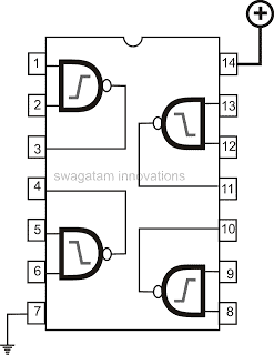
One such device is the IC 4013, which is basically a dual D-type flip flop IC, and may be used discretely for implementing the proposed actions.
In short the IC carries two in built modules which may be easily configured as flip flops just by adding a few external passive components.
IC 4013 Pinout Function
The IC may be understood with the following points.
Each individual flip flop module consists of the following pin outs:
- Q and Qdash = Complementary outputs
- CLK = Clock input.
- Data = Irrelevant pin out, must be either connected to the positive supply line or the negative supply line.
- SET and RESET = Complementary pin outs used for setting or resetting the output conditions.
The outputs Q and Qdash switch their logic states alternately in response to the set/reset or the clock pin out inputs.
When a clock frequency is applied at the CLK input, the output Q and Qdash change states alternately as long as the clocks keep repeating.
Similarly the Q and Qdash status can be changed by manually pulsing the set or the reset pins with a positive voltage source.
Normally the set and the reset pin should be connected to the ground when not utilized.
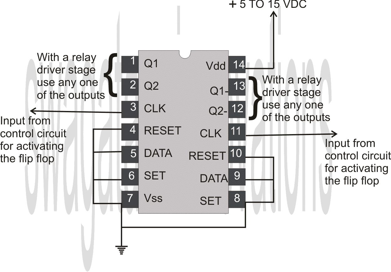
The following circuit diagram shows a simple IC 4013 set up which may be used as a flip flop circuit and applied for the intended needs.
Both may be utilized if required, however if only one of them is employed, make sure the set/reset/data and clock pins of the other unused section is grounded appropriately.
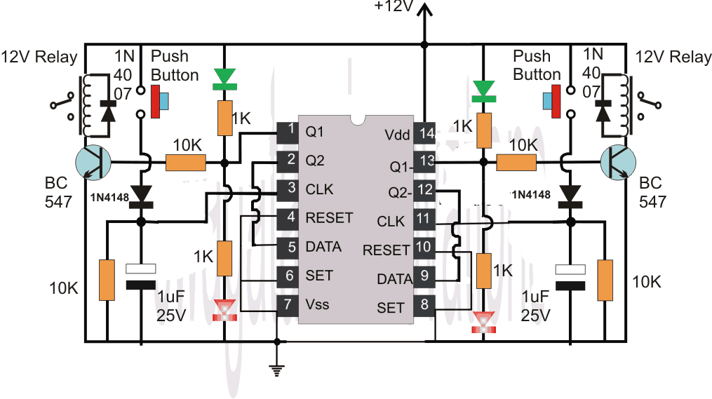
A practical application flip flop circuit example can be seen below, using the above explained 4013 IC
Mains Failure Backup and Memory for the Flip Flp Circuit
If you are interested to include a mains failure memory and back up facility for the above explained 4013 design, you can upgrade it with a capacitor backup as shown in the following figure:
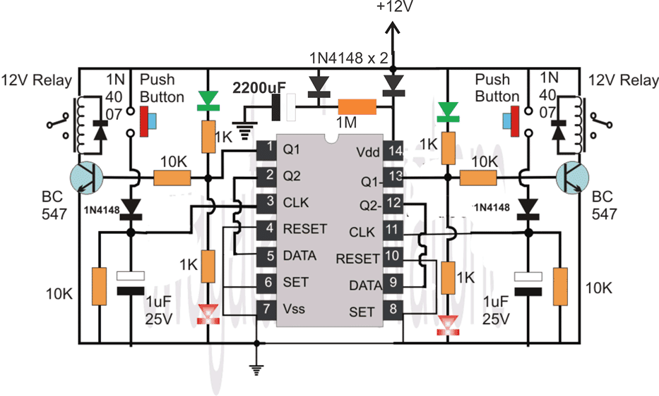
As can be seen, a high value capacitor and resistor network is added with the supply terminal of the IC, and also a couple of diodes to ensure that the stored energy inside the capacitor is used for supplying only the IC and not to the other external stages.
Whenever mains AC fails, the 2200 uF capacitor steadily and very slowly allows its stored energy to reach the supply pin of the IC keeping the IC's "memory alive" and to make sure that the latch position is remembered by the IC while the mains is unavailable.
As soon as the mains returns, the IC delivers the original latching action on the relay as per the earlier situation, and thus prevents the relays from losing its previous switch ON status during the mains absence.
4) SPDT Electronic 220V Toggle Switch using IC 741
A toggle switch refers to a device which is used for switching an electrical circuit ON and OFF alternately whenever required.
Normally mechanical switches are used for such operations and are extensively employed wherever electrical switching is required.
However mechanical switches have one big drawback, they are prone to wear and tear and have the tendency of producing sparking and RF noise.
A simple circuit explained here provides an electronic alternative to the above operations. Using a single op amp and a few other cheap passive parts, a very interesting electronic toggle switch can be built and used for the said purpose.
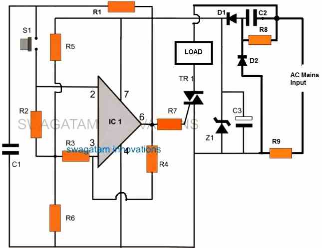
Though the circuit also employs a mechanical input device but this mechanical switch is a tiny micro switch which just requires alternate pushing for implementing the proposed toggling actions.
A micro switch is a versatile device and very much resistant to mechanical stress and therefore does not affect the efficiency of the circuit.
How the Circuit Functions
The figure shows a straightforward electronic toggle switch circuit design, incorporating a 741 opamp as the main part.
The IC is configured as a high gain amplifier and therefore its output has the tendency of easily getting triggered to either logic 1 or logic 0, alternately.
A tiny portion of the output potential is applied back to the non inverting input of opamp
When the push button is operated, C1 connects with the inverting input of the opamp.
Assuming the output was at logic 0, the opamp immediately changes state.
C1 now begins charging through R1.
However keeping the switch pressed for a longer period of time will only charge C1 fractionally and only when it’s released does C1 begins charging up and continues to charge up to the supply voltage level.
Because the switch is open, now C1 gets disconnected and this helps it to “retain” the output information.
Now if the switch is pressed once again, the high output across the fully charged C1 becomes available at the inverting input of the op amp, the op amp yet again changes state and creates a logic 0 at the output so that C1 starts discharging bringing the position of the circuit to the original condition.
The circuit is restored and is ready for the next repetition of the above cycle.
The output is a standard triac trigger set up used for responding to the outputs of the opamp for the relevant switching actions of the connected load.
Parts List
- R1, R8 = 1M,
- R2, R3, R5, R6 = 10K,
- R4 = 220K,
- R7 = 1K
- R9 = 22 ohm 2 watt
- C1 = 0.1uF,
- C2,C3 = 470uF/25V,
- S1 = micro-switch Push Button,
- IC1 = 741
- Triac BT136
- D1, D2 = 1N4007 Diodes
IC 741 Flip Flop using Set/Reset Touch Pads
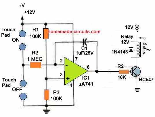
A 741 IC can be also used to create a set/reset type of flip flop circuit, using two sets of touch pads.
As shown in the above figure, the upper sets of touch pads can be used to trigger ON the 741 output which in turn switches ON the relay driver stage and the load.
When the lower pair of touch pads are touched the IC 741 is resets to its original condition causing the output to the relay driver stage to turn OFF.
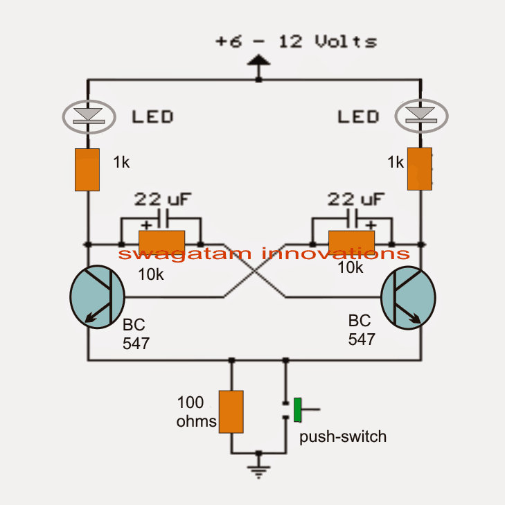
5) Transistor Bistable Flip Flop
Under this fifth and last but not the least fliop flop design I have explained a couple of transistorized flip flop circuits which can be used for toggling a load ON/OFF through a single push button trigger.
These are also called transistor bistable circuits.
The term transistor bistable refers to a state of a circuit where the circuit works with an external trigger to render itself stable (permanently) over two states: ON state and OFF state, hence the name bistable meaning stable on either ON/OFF states.
This ON/OFF stable toggling of the circuit alternately could be normally done through a mechanical push button or through a digital voltage trigger inputs.
So I have explained the proposed bistable transistor circuits with the help of the following two circuit examples:
Circuit Operation
In the first example we can see a simple cross coupled transistor circuit which looks quite similar to a monostable multivibrator configuration except the the base to positive resistors which are missing here intentionally.
Understanding the transistor bistable functioning is rather straightforward.
As soon as power is switched ON, depending upon the slight imbalance in the component values and the transistor characteristics, one of the transistor will switch ON completely rendering the other to switch OFF completely.
Suppose we consider the right hand side transistor to conduct first, it will get its biasing via the left hand side LED, 1k and the 22uF capacitor.
Once the right hand side transistor has switched completely, the left transistor will switch OFF completely since its base will now be held to ground via the 10k resistor across the right transistor collector/emitter.
The above position will be held solid and permanent as long as power to the circuit is sustained or until the push-to-ON switch is depressed.
When the the shown push button is pushed momentarily, the left 22uF capacitor now will be unable to show any response since its already fully charged.
However the right 22uF being in a discharged state will get an opportunity to conduct freely and provide a harder biasing to the left transistor which will instantly switch ON reverting the situation in its favor, wherein the right hand side transistor will be forced to shut off.
The above position will be held intact until the press button is yet again pressed. The toggling can be flipped alternately from left to right transistor and vice versa by actuating the push switch momentarily.
The connected LEDs will light up alternately depending upon which transistor is rendered active due to the bistable actions.
Circuit Diagram
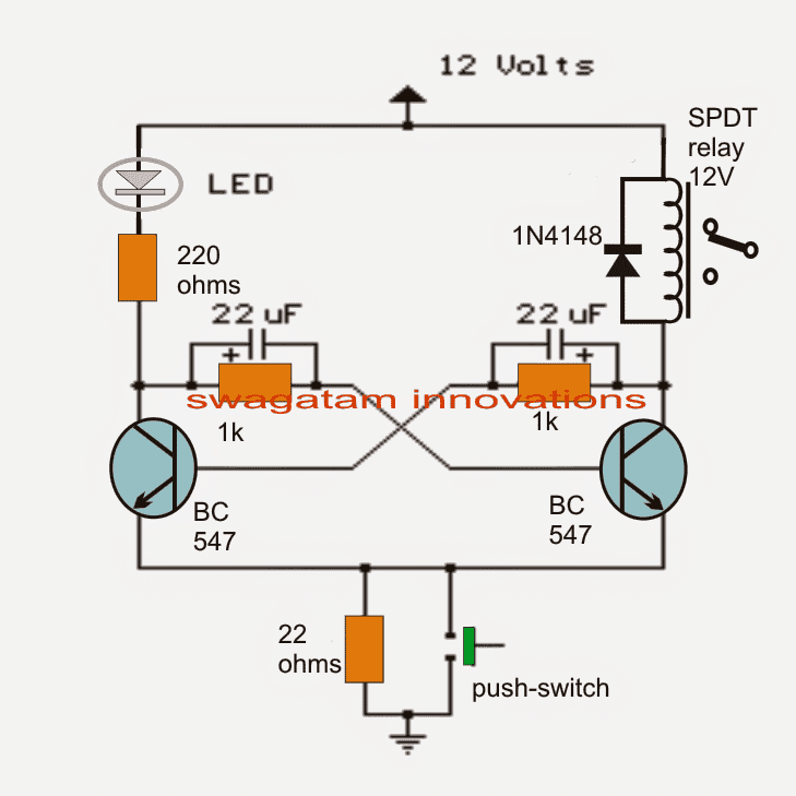
Transistor bistable flip-flop circuit using a relay
In the above example I have explained how a couple of transistors can be made to latch in bistable modes by pressing a single push button and used for toggling relevant LEds and the required indications.
In many occasions a relay toggling becomes imperative in order to switch heavier external loads.
The same circuit which is explained above can be applied for activating a relay ON/OFF with some ordinary modifications.
Looking at the following transistor bistable configuration we see that the circuit is basically identical to the above except the right hand LED which is now replaced with a relay and the resistor values have been adjusted a bit for facilitating more current that may be required for the relay activation.
The operations of the circuit is also identical.
Pressing the switch will either switch OFF or switch ON the relay depending upon the initial condition of the circuit.
The relay can be flipped alternately from an ON state to OFF state simply by pressing the attached push button as many times as desired for switching the external load connected with the relay contacts accordingly.
Bistable Flip Flop Image
Do you any more ideas regrading flip flop projects, please do share with us, we'll be most glad to post them here for you and for the pleasure of all the dedicated readers.
Flip Flop Circuit using IC 4027
After touching the touch-finger pad. Transistor T1 (a type of pnp) begins to operate. The resultant pulse at the 4027 's input clock has extremely sluggish edges (due to CI and C2).
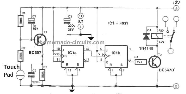
Accordingly (and extraordinarily) the first J -K flip-flop in 4027 then serves as a Schmitt control gate turning the very sluggish pulse at its input (pin 13) into a smooth electrical signal that can be added to the next flip-flop's clock input (pin 3).
Afterwards the second flip-flop functions as per the textbook, providing a real switching signal which can be used to turn a relay on and off through a transistor stage, T2.
The relay conducts alternately if you tap the contact plate with your finger.
The circuit current consumption while the relay is off is less than 1 mA, and when the relay is on, up to 50 mA. Any relay that is more affordable can be used for as long as the coil voltage level is 12 V
However use a relay with correctly rated contacts when operating a mains device.
Using IC 4049
Set-Reset Flip Flop Using IC 4011
CMOS IC's feature several benefits above TTL. One of the key features being the high input impedance. In the following figure, a couple of NOR gates are connected across each other with a cross coupled configuration to create a flipflop.
When touch plate S is touched background noise develops an AC voltage at G1 input. In the course of the first positive cycle G1 output turns negative which causes the flipflop to SET, switching ON the relay RLA1 on. This continues to be on as long as the R plate or the RESET plate is not touched.
R1 and R2 should not be removed given that they discharge any voltage levels developed on the plates soon after they are touched, hence enabling the flipflop to get its state altered swiftly.
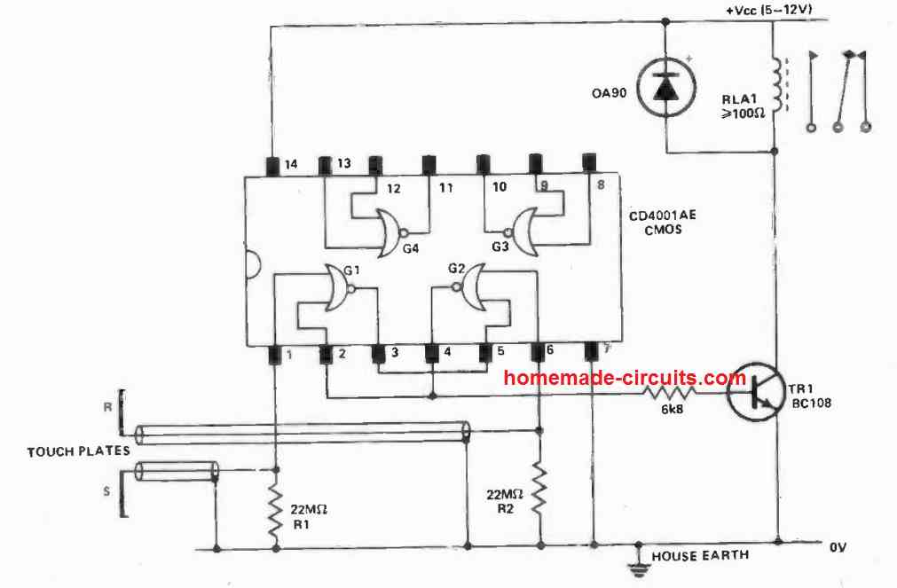
R1 and R2 additionally protect against any static charges racking up, which can cause damage to the IC, when the supply is in the disconnected condition.
The 22Mohm resistors can be hard to obtain therefore a pair of 10 Mohm resistors can be connected in series.
The flip flop circuit could be kept switch ON continuously since a milliameter reveals absolutely no current being consumed in the relay off position.
In case relay RLA1 is removed TR 1 collector turns into a TTL output having a high fan out.
Attach the inputs of G3 and G4 to ground in case these are kept unused. The touch plates could be positioned many feet away from the IC only if shielded termination is used for the connecting wires.
Miscellaneous Flip Flop and Set/Reset Circuits
The following paragraphs explain a few more easy to build flip flop circuits using CMOS gates and op amp.
The first circuit uses a single buffer gate from the IC 4050. The second circuit uses a couple of gates from the IC 4011
Using a Single Buffer gate
A simple flip flop or set reset circuit can be easily built using a single buffer gate, such as from the IC 4050.
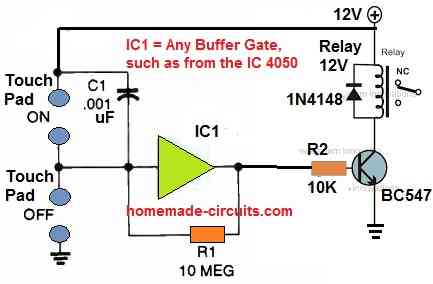
As shown in the above figure you just need a 10 M resistor and a couple of touch pads to configure the proposed flip flop circuit.
A relay driver stage can be seen attached with the output of the flip flop for activating the ON/OFF action of the load in response to the finger touch.
Set/Reset Flip Flop Circuit Using Two NAND Gates
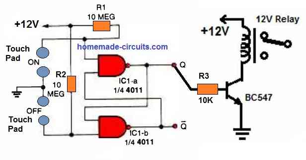
If you have just a couple of NAND gates from an IC such as 4011, then you can easily build a nice little set/reset flip flop circuit as depicted in the above figure.
Touching the upper set of touch pads sets the flip flop, so that the relay driver is switched ON.
Touching the lower set of touch pads resets the flip flop such that the relay driver is switched OFF.
Warning: Please do not forget to connect a freewheeling diode across the relay coil for safeguarding the transistor
Set/Reset Flip Flop Circuit using a Single 4011 IC
If you don't like the use two sets of touch pads and are looking for a flip flop set/reset circuit with a single set of touch pads, then the following circuit will be perfect for your need.
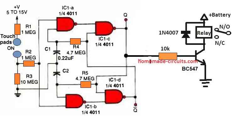
When the touch pads are alternately touched and released, the outputs Q and Qbar alternately toggle high and low creating a set/reset operation across the outputs. The relay driver stage is toggled ON/OFF accordingly.
Comments
Hello there
I am looking for a way to switch on two 12v circuits using a momentary press switch. The circuit needs to be off until the switch is pressed, first circuit on with the first press, second circuit on/ first circuit off with the second press and all off again on the third press.
The circuit is for a car heater to control 2 speeds of the fan, slow speed is through a resistor and fast speed is direct to the motor.
Is there a ready made switch circuit to do this or is it possible to make one, even for a novice.
Thanks in advance.
Hi, you can try the following design, it should do the job for you, you can assemble it yourself at home:
https://www.homemade-circuits.com/wp-content/uploads/2025/02/IC-4017-flip-flop-two-loads-ON-OFF-with-single-pushh-button.jpg
Thank you for the circuit diagram, I will source the parts and make it. Another couple of queries though.
I don’t know the wattage of the motor but it has a 25amp fuse to protect the circuit so will this survive the current to power the motor or would it need to have the outputs to a relay?
If it will power the motor without needing relays will the outputs need diodes to stop a back feed into ic 4017? This is because the two speeds are power feeds before a resistor for slow speed and after the resistor for fast speed so they are technically connected together.
Once again thank you for your time and expertise.
Regards
Johnny
Sure, no problem.
Is the motor DC?
If it is DC then you can use current-controlled MOSFET stages for getting the intended current optimized outputs for the Motor speed control.
Hello Sir. Can 74LS74 also be used as a alternative for CD4013?
Yes it can be used, but the supply voltage must not exceed 5V
Hello Swagatam,
I am looking for a circuit with a single touch plate to cycle through the START, STOP AND RESET functions of two CD4017 Ic’s. For simplicity, in the first 4017, only the clock enable is utilized as the reset is tied to the ground. This is optional.
Any help you could give me is greatly appreciated.
Cheers
Hi Davis,
yes that’s definitely possible, however the start, stop, reset functions can be only implemented sequentially, meaning the first touch will start the circuit, the second touch will stop it and the third touch will reset it.
Thanks for the quick response. It is greatly appreciated. I would want them sequential exactly as you stated.
Ok, i will design it for your, however two 4017 ICs would be required for implementing the mentioned operations. One 4017 will handle the touch operations for triggering the start, stop, reset for the other 4017.
Let me know if this suits your requirement or not….
In the circuit using opamp 741 and triac, why do jou requure C3 to be 400v compliant. It is parallel to the opamp supply which is surely not 400v capable.
I expect C3 to be 25v capable and to in order to lower supply ripple to be 470uf instead of 470nf.
C3 was rated at 400V for extra safety since it is directly linked with C2 and considering a situation where the zener diode somehow gets damaged. However if the zener diode gets damaged it will create a short circuit. So yes the capacitor C3 can be a 25V capacitor and for better filtration it could be a 470uF.
I have corrected the diagram and the parts list appropriately, you can check it out.
Good sir, I have a problem and do not know if a solution exists. I am adding some multi-functional lights to my vehicle (12v system, negative ground). The lights have 2 functions. F1 is a steady light, F2 is a strobing light. The only way to change the mode is by applying and removing 12v (these lights do not have a memory circuit, or a 3rd wire to control function). I would like these light, when powered, to always be in F2 (strobe). The lights will be powered by an On/Off toggle (this cannot be changed with the hardware being installed). Is there a way, when the switch is closed, to send 12v to the light (maybe 0.25 – 0.50 seconds), open the circuit, and close the circuit? It kind of sounds like a variation of a flip-flop, I just need it to not flop-flip.
When switch is closed, a 12V must enter the circuit after 0.5 seconds, then it must switch OFF, and then switch ON again…I can’t seem to figure out the circuit, it looks difficult to me.
I have designed a flip flop circuit with transistor BC547, with 22LEds (11 in each series), it is not functioning with transformer less power supply.Pl. help.
Did you use proper filtration and a regulator for your transformerless power supply? Use a 2200uF/50V capacitor for the filter capacitor and use a transistor/zener diode regulator for stabilizing the circuit output, then it might work.
Hi,
I was looking for the same circuit like Mr Dheeraj have asked. First of all I would like to tell you that, I am not from electronics back ground, and I make circuit, and try to learn as a hobby.
I have few doubts. Pin 16 of IC4017 is VCC pin. in the modification of the circuit, where push button has been removed, how the IC is getting required VCC. Because the circuit is getting direct AC Volt as input.
2nd, a red colour Diod is connected with BT136 and Pin 2 after 1K Resistor. Is that a LED?
3rd, what are the watt value of the 1K, 10K, 1M Resistors used in the design.
4th, Any electrolytic capacitors will work or else I have to use any specific. If specific, please tell me.
5th BT136 have three legs. Can you please help me with providing the leg details? Or any specific BT136 details?
I am waiting for your kind response.
Thanks & Regards
Raju Saha
Hi, here are answers to your questions:
In the “Electronic Switch without Push Button”, the ON/OFF switch is used for sequencing the 4017. Initially while the switch is in the ON position, the 2200uF capacitor is charged. When the switch is momentarily turned OFF, the IC 4017 remains switched ON via the 2200uF charge, and therefore any subsequent ON/OFF switching enables the required sequencing of the 4017 IC via the BC547 transistor.
Yes, those red colored diodes are LEDs to indicate which triac is switched ON.
All the resistors are 1/4 watt rated.
Any standard electrolytic capacitor will work for the polarized capacitors.
The BT136 is connected in the following manner:
If you hold the printed side of the BT136 facing towards you,
The extreme right side leg is the gate which goes to the LED
The extreme left side left is connected with the ground or the negative Dc supply line.
The center leg goes to the load or the lamp.
The entire circuit is not isolated from mains 220V so be very careful while testing or handling the circuit in switched ON and uncovered condition.
Hi,
Thank you very much for your reply. I will make the circuit now, and let you know. I have requested you about the information on making of addressable devices, somewhere in your another post. But I am not able to find that one. Did you provided any reply on that?
Looking for your kind response.
Thanks again.
Hi, you had posted the previous question under the following article:
https://www.homemade-circuits.com/adjustable-0-100v-50-amp-smps-circuit/
Thank you very much for your kind response. I will let you know whether I am able to make that or not.
Thanks again
I am glad to help!
Hi Swagatam,
I have tried to make the circuit of Mr Dhiraj, and Failed 3 times. Then I started the article written by you, Understanding the pins of IC 4017, and found, when the IC 1st start, the Pin 3 goes high 1st, then pin2 and so on. But in your schematic, pin2 has been used as 1st initial actuation. My question is why? Where as it should be pin3.
I was trying to actuate 5 v dc relay, instead of ac load. So I removed the 12v zener diod part, as already I am using DC12v as input to the IC. Am I correct? Please rectify me.
The Clock signal at Pin 14. This is the very confusing part, that I did not have any confidence. How BC547 npn transistor provide clock pulse. Also I have removed BT 136, as my requirement is actuation of 5v dc relay. So I have used pnp transistor. Am I correct?
What is actually a clock signal.
Waiting for your reply.
Thanks in advance.
Hi Raju, the circuit will work but it will need some adjustments.
In your modified design you must use an NPN transistor as shown in the first diagram.
A clock signal is nothing but a positive supply voltage pulse fed to pin14. It means the pin14 needs to be initially grounded with a resistor, then as soon as you add a positive voltage to pin14 it accepts it as a clock pulse. Again when you remove the positive voltage from pin14 it becomes 0V through the ground resistor, and when you once again apply the 12V it accepts it as a second clock pulse and so on. For every clock pulse the output shifts from pin#3 to pin2, to pin4 and until it reaches to pin11.
The BC547 works in this way. As soon as you switch ON power the 2200uF capacitor charges and remains charged. The IC is reset via 0.1 uF capacitor and an output positive high hangs at pin#3, which we don’t need initially that is why pin#3 is kept blank.
After this when you turn OFF the switch the entire circuit switches OFF but the IC 4017 remains active due to the 2200uF capacitor charge. Now, when you turn ON the switch again, the voltage enters the BC547 base via the 1uF and triggers it momentarily, which causes the supply voltage to enter through the collector/emitter of the transistor and hit pin#14, which sends a clock pulse to pin14 and causes the IC to trigger with the clock and its output shifts from pin#3 to pin#2 and this goes on happening as many times as you press the switch ON OFF
I hope I could explain the functioning properly to you.
3) Flip Flop Circuit using IC 4013: Who is using this circuit in 2022?
I’ve built this circuit with an CD4013B (TI chip), but I cannot get it to work.
CD4013B datasheet noted Vin is 3Vdc up to 18Vdc. (20Vmax absolute)
Noted startup state: (voltage first applied to circuit)
Q1 = High
Q2 = Low
When the pushbutton is pressed momentarily, Q1 and Q2 will change states, but always go back to default state.
the Q1 output never stays latched on at Low. if I start pressing the pushbutton randomly, sometimes, it will actually change stated and stay (Q1=Low, Q2=High).
most other times, it never actually changes and stays.
I have noted that the circuit works somewhat correctly and consistently when Vin is ~5Vdc. However, even at 5Vdc, the states sometimes still go back to start up state.
Thanks for your feedback!
Agustin
Actually, i just built that same circuit!
And i also experiencing the same thing.
I want to build a 2 amp separate control, and wanted to start the state as off both. So i thought okay, let’s default the “red” led part, and just leave out the “green led” parts.
I was thinking i would use a bc557 and connect the relay towards ground instead too.
But as i power it up, it is off. One short button press, it switches and stays on the second phase. But every button press it goes back to original state only while the button is closed. As soon as i leave my finger it jumps back.
I am driving it with 12V
You can try connecting the reset pins to ground via a 10K resistor, and then connect a small value capacitor such as 1uF/25V between the positive line and the reset button. With this arrangement each time power is switched ON, the short pulse through the capacitor will reset the IC to zero and ensure that the output pins always start with a zero logic.
Your button press maybe causing debouncing effect, you can try increasing the 1uF capacitor value at the CLK pins to 10uF and see if that helps to correct the debouncing effect.
Thank you for your fast reply and helping! I tried with 10uF, but nothing changed, except it sometimes not switching at all. i thought about the debouncing effect, which is a big issue with most of the flip-flop circuits. At least for me. I tried so many circuits, only transistor ones, 555 types, all of them were “glitching out”. My only successful circuit was with 4017 IC. But that can control only one relay sadly.
We want the capacitor at the clock input to charge slowly to avoid the bouncing effect. For this you can try the following modifications:
Let the 1uF be as it is at the CLK pin#3 and pin#11 of the IC.
Replace the 10K resistor at the CLK pin with a 100K resistor.
Next, connect a 10K resistor in series with the push button switch. The 10K will cause the CLK capacitor to charge slowly and should help to prevent the switch bouncing effect.
Thank you for your kind help, unfortunately it didn’t made any effect, working the same way. I am not sure about the button’s bouncing effect may causing this phenomena. With the base circuit, the led turns off as i press and hold the button. And as i release that it turns back on. Regardless of the speed of the on/off changes, it does it precisely. Also i have CD4013BP, this type i couldn’t find a datasheet for. I don’t know if that matters, i believe the B ending is indicating that the outputs are buffered.
4013 and 4017 are both CMOS ICs so their clock inputs must behave exactly the same way….if it is working for you with 4017 then it should have worked for 4013 IC also. Not sure why it is not working with 4013. What you are experiencing looks exactly like a switch bounce effect. However it may be due to some other issue also, can’t figure it right now.
I don’t think the ending suffix of the IC might be anyway related to this issue. You can refer to this datasheet, it should be applicable to all 4013 ICs.
https://www.ti.com/lit/ds/symlink/cd4013b.pdf
Oh okay, i was mistaken a bit with info, i apologize. I am at work atm, but i gladly i have one circuit with me, and it is driven with 4011.
I built an IR switch with 4017 tho. Still i was able to switch it with button too. But that is at home, i cannot check it out.
This is the circuit what i use for the 4011 currently:
https://ibb.co/L5VZPvg
I also using 5V instead of 12V. I have much more relays for 5V than 12V.
OK thanks, however, the link is not working, it is showing “this site can’t be reached” may be you can try uploading it to some other free image hosting site. I will check it out.
Oh, sorry! I don’t use these sharing sites like ever. 🙂
I hope this will work:
https://www.homemade-circuits.com/wp-content/uploads/2022/09/4011-flip-flop-circuit.jpg
It looks good, the 1M and the 1uF are probably the ones which are controlling the switch bounce.
Maybe i will try with 1M resistor as well.
Trying to do some experiment.
Sure, no problem. Keep us posted.
Okay, now this is getting stranger 😀
I replaced the 10K resistor parallel with the 1uF capacitor to 1M resistor. Now it works as the following:
One button press: switches to the opposite state.
Second btn press: switches back to starting state, but after 1 second it automatically switches back to the second state.
I am completely puzzled!
That’s puzzling indeed! You can try putting the switch parallel to the 1uF capacitor instead of at the top and see how it works?
Addendum: without the cap, only resistor it works but 30% of times the button bouncing is present. But with any cap it goes to the switch off then 1 sec later switching back on thing.
Well it was a good experiment, first i just tried to put another button parallel to the cap and resistor, made no difference.
Then i removed the resistor, so only the cap left with the extra button parallel with it.
So when i pressed the main button, it turned on, but then no matter how many times pushed the same button, nothing happened. (obviously, because no data triggered inside the ic)
But as i pressed once the extra button then the main button switched off the led and it stayed that way. (I am just testing one side)
It seems nothing is working which shouldn’t be the case, because the CLK input of the IC is just a simple CMOS input which can be managed with a resistor and a capacitor. Now I am wondering is the IC good, could there be a problem in the IC itself. If the RC network can work with 4017 CLK input, then why not with a 4013?
Well i tried with another IC,but it acted the same way. I have no idea what can be the issue.
This is the circuit i am using for 4017 IR version.:
A button shorting the IR signal legs are working as well.
Yes the 4017 version looks normal! Still can’t figure out why the CLK of 4013 is not working with a push button switch for you? I found another circuit which uses a 4013 along with a 555 IC, you could probably try it and see how the 4013 responds to a 555 output.
Actually at this point i usually give up 🙂
Also i try to go to the least amount of components, in this case it’s probably solves the issue at hand, but i would go with another method.
I made an extended schematic and pcb draw on 4011, so i think the same method can be achieved with the other IC. I just built it and it works. Tho the amount of relays draw much more power.
These circuits most probably must be corrected or extended.
https://www.homemade-circuits.com/wp-content/uploads/2022/10/4011-push-button-flip-flop.jpg
https://www.homemade-circuits.com/wp-content/uploads/2022/10/4011-flip-flop-PCB-design.jpg
OK no problem, I can understand!
Your 4011 based circuit actually looks good, I hope the readers will find it very helpful.
All the best to you!
I thank you all your help and time and energy to try to solve this phenomena. I am sorry that we couldn’t find out what is causing really that strangeness!
Thank you also for these awesome circuits you posting here!
All the best to you too, Sir! 🙂
Thank you so much, the pleasure is all mine!
No problem, Sylvester!
Thanks Swagatam. I will experiment with that and get back to you.